Fine-Pitch Chip Removal and Adapter PCB Design
Lift the main chip off a retro handheld console, solder it onto a PCB we drew ourselves, wire it back through a ribbon cable — and the job is only done if the console still runs.
- Role
- Course Project · Team of four
- Period
- Sep. 2024 – Jan. 2025
- Institution
- SUSTech Supervised by Dr. Guang Wu
Why this matters
Everything hard about this sits outside the schematic. The chip has 44 pins at 1.27 mm pitch and all its solder hides underneath it; one careless pass with a hot air gun lifts a pad clean off the board, and a lifted pad means a dead console. Get the board wrong and you wait a week for the next fabrication run. So the real subject was never whether you can drive an EDA tool — it was the things not written in the textbook: how to get a chip off intact, how to solder 1.27 mm pins without bridging them, and why the PCB design rules say what they say.
What I did
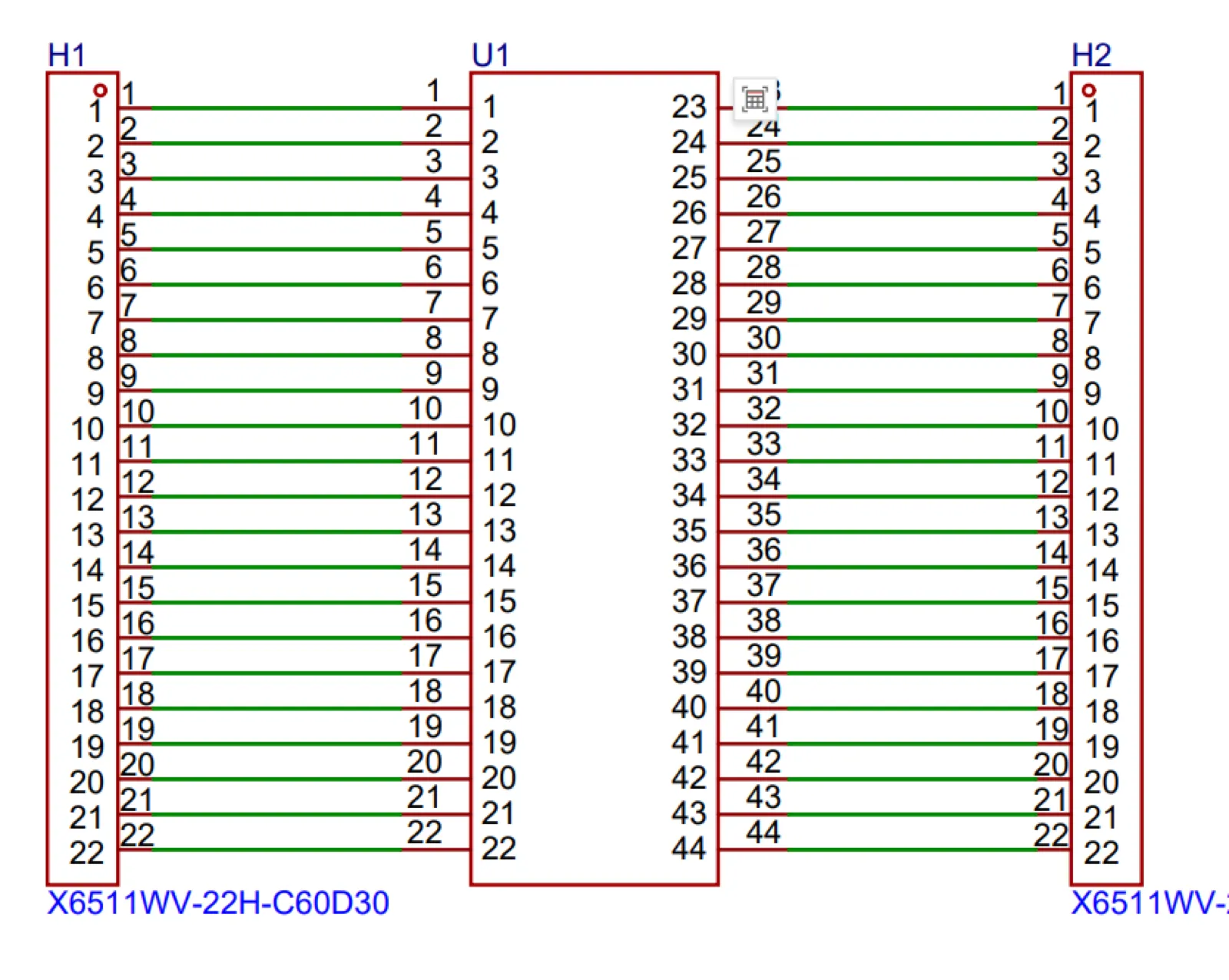
- Measured the chip with calipers — 22 pins per side, 28 mm long — giving a 1.27 mm pitch; chose 2.54 mm headers to suit the ELVIS breadboard, with 61 mm between rows.
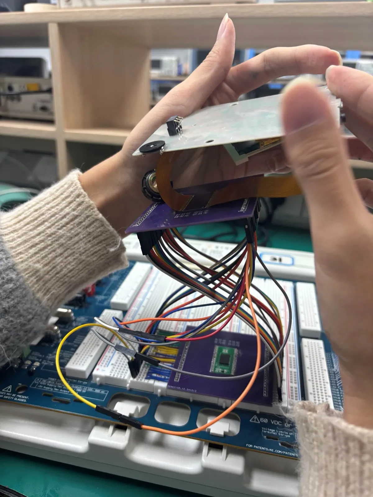
- Drew the schematic and PCB in LCEDA, fanning all 44 chip pins out to two 22-pin headers, and sent it out for fabrication.
- Soldered three different ways: spot soldering for the 2.54 mm headers, solder paste and hot air for the 1.27 mm chip pins, and hand soldering from both ends inward for the ribbon cable, whose insulation will not survive sustained heat.
- Traced faults pin by pin on NI ELVIS: resistance mode to find bridges between adjacent pins, continuity mode to find cold joints between pad and pin.
- When one console powered up dark, swapping the display changed nothing; testing showed an indicator LED lit regardless of whether the chip was present, which located the fault in the motherboard rather than the chip.
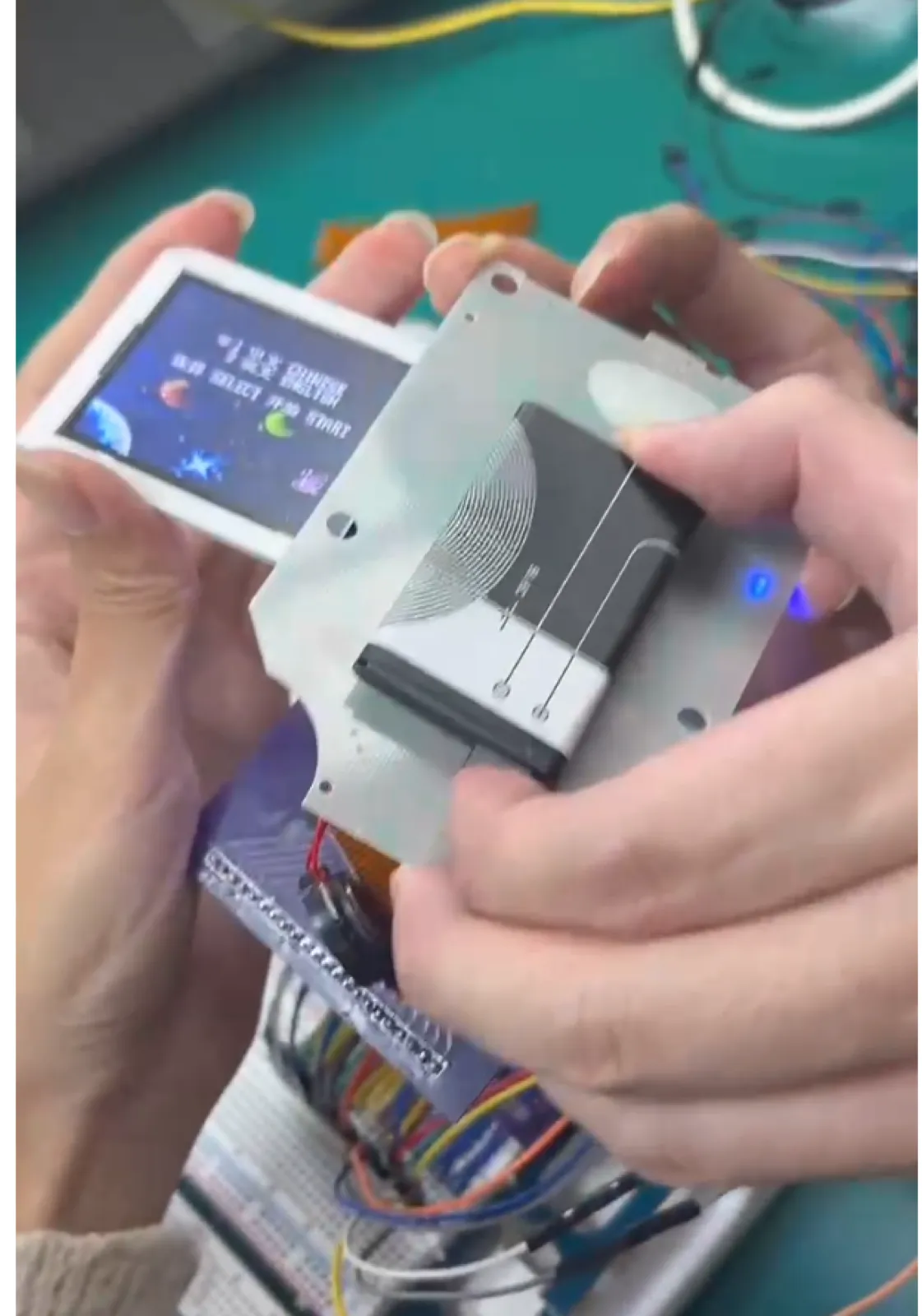
A four-person digital circuits course project built around a retro handheld console: lift the chip off its original board, design an adapter PCB, solder the chip onto that, and wire it back to the motherboard through a ribbon cable — with the console still working at the end.
Outcome
- The chip was successfully transplanted onto our own adapter board and the console powered up and ran again.
- The removal technique was worked out by trial: high temperature, low airflow, sustained heating, and lifting straight up with no sideways prying. Iron-and-wick attempts had all failed because the solder sits underneath the package. The fallback our instructor offered — scraping the board to expose copper and bridging with 0.38 mm wire — restores function but sacrifices the pads.
- The first fabrication run came back unusable: inconsistent trace widths and spacing, an asymmetric layout, an oversized board, and right-angle traces. The second revision followed the rules — 45° or curved bends, symmetric layout, tightened outline, DRC before submitting — and that is the one we used.
Technologies
- LCEDA
- PCB Design & Fabrication
- Hot Air & Hand Soldering
- NI ELVIS
- Circuit Debugging